
European Conference on Energy
Dispersive X-Ray Spectrometry
EDXRS 2002
June 16 to 21, 2002 in Berlin, Germany.
|
June 16 to 21, 2002 in Berlin, Germany. |
|
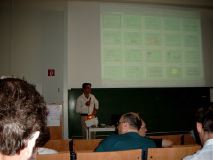
From the Book of Abstracts of EDXRS 2002 Conference, Berlin, Germany, p. 16.
Hakob P. Bezirganyan and Siranush E. Bezirganyan, Faculty of Physics, Yerevan State University, #1, A. Manoogian Street, Yerevan 375025, Armenia; Si-based optoelectronic devices need to be monolithically integrated with Si-based microelectronics and
operate in the infrared wavelength region, suitable for fiber-optic
communications. To achieve an efficient photo-response at the 1,3 mm wavelength region with SiGe/Si photodetectors,
the Ge concentration should be in excess of 35%. The lattice constant
of Ge is 4,2% larger than that of Si. Therefore if a bulk Ge
layer is placed on a bulk Si layer in an attempt to form a single
crystal, every 24th Si atom at the interface would not be able to
form a bond with a Ge atom. The lattice mismatch between Si
and Ge constrains the design of SiGe heterojunction devices
because of the limited thickness for pseudomorphic SiGe epilayers on a
Si platform, i.e. there exists a maximum thickness called the critical
thickness above which is necessary too much energy to strain additional layers
of material into coherence with the substrate. As the result a defects, e.g. a
misfit dislocations, appear in the system to relieve the strain (see figure 1).
strain - compensated misfit dislocation Incorporation of C into Si1-aGea layer to form ternary
Si1-a-b GeaCb
alloy makes it possible to reduce the compressive strain between the SiGe
epilayer and the Si substrate, and therefore to control the strain about the
lattice matching condition for Si substrates [1-4]. If (a / b) ~ 10, then the
lattice constant in the growth direction is equal to that of the substrate [1].
The proposed model of the Si1-a-b GeaCb / Si strain-compensated
heterojunction is presented in the figure 1. The strain-compensated Si1-a-b GeaCb
thin layer and the silicon substrate have the same value
of the spacing period along the growth surface - the entrance surface of the
x-rays according to this model. However, there exists a shift between their
space periods stipulated by a misfit dislocations (see figure 1). The
investigations, sensitive to the phase shift, can be performed using the
Grazing-Angle Incidence X-ray Backdiffraction (GIXB) technique, i.e. the x-ray
diffraction in the conditions, when the Bragg angle is more than one or two
critical angles of incidence [5]. It is considered theoretically the GIXB
depending on the values of phase shift between the space periods, and of the
Bragg angle. B. Dietrich, H. J. Osten, H. Rucker, M. Methfessel, and P. Zaumseil, Phys. Rev. B, 49
(1994), 17185. J. Kolodzey, P. R. Berger, B. A. Orner, D. Hits, F. Chen, A. Khan, X. Shao, M. M. Waite, S. Ismat Shah, C. P. Swann, and
K. M. Unruh, J. Cryst. Growth, 157 (1995),
386. X. Shao, Ralf Jonczyk, M. Dashiell, D. Hits, B. A. Orner, A.-S. Khan, K. Roe, J. Kolodzey, P. R. Berger, M. Kaba, M. A.
Barteau, and K. M. Unruh, J. Appl. Phys., 85 1
(1999), 578. A. P. Bezirganyan and P. A. Bezirganyan, Phys. Stat. Sol. (a), 105 (1988),
345. | |||||||||||||||||||||||||

|
|
|
|
|
|

|

|
|
|
|
|
|
|
|

|
|

|

|
|
|

|

|

|

|
|
|
|
|
|
|
|
|
|
|

|
|
|

|

|

|

|

|

|
|
|

|

|
|

|

|
|
![]()
to Dr. Hakob BEZIRGANYAN's Page
|
Created: |
July 07, 2002. |
|||
|
Last updated: |
July 12, 2002. |
|||
